 |
Moteur de recherche de fiches techniques de composants électroniques |
|
|
Moteur de recherche de fiches techniques de composants électroniques |
|
The question interval is too short.
Please try again in a few seconds.

Hello, Please ask a question about AD795 Datasheet
# Example questions:
➢ What type of circuit is illustrated in figure 27, and what does '–vs' likely represent in that circuit?
➢ How does temperature affect the short-circuit current limit?
➢ What is the relationship between supply voltage and quiescent supply current?
| Part No. | AD795 |
| Manufacturer | AD |
| Size | 435 Kbytes |
| Pages | 20 pages |
| Description | Low Power, Low Noise Precision FET Op Amp |






1. Device:
️· The document pertains to the AD795 – an unspecified integrated circuit (likely an operational amplifier or similar analog device).
2. Key Characteristics & Performance Metrics:
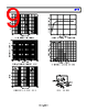
️· Frequency Response: The AD795 has a defined frequency response, including open-loop gain and phase margin (Figure 30). It's suitable for applications involving frequency-dependent signals.
️· Harmonic Distortion: Total Harmonic Distortion (THD) is characterized up to certain frequencies (Figure 31).
️· Output Impedance: The closed-loop output impedance is defined (Figure 32).
️· Quiescent Current: The quiescent (idle) supply current varies with the supply voltage (Figure 34).
️· Input Offset Voltage: There's a distribution of input offset voltages, which needs to be accounted for in applications requiring high accuracy (Figure 35).
️· Supply Voltage Range: The device's behavior changes with supply voltage (Figure 33, Figure 34).
️· Power Supply Rejection: The device has a specified Power Supply Rejection Ratio (PSRR) which measures its ability to filter out unwanted power supply noise (Figure 36).
️· Common-Mode Rejection: The Common-Mode Rejection Ratio (CMRR) is also defined, indicating the device's ability to reject common-mode signals (Figure 18).
️· Large Signal Response: Defined for a specific configuration (RL=10k ohms, VIN = 3V) (Figure 22)
️· Unity Gain Inverter: A basic circuit configuration (Unity Gain Inverter) is presented (Figure 27).
3. Specific Values & Conditions (Examples):
️· Load Resistance (RL): RL=10kΩ is mentioned in multiple contexts.
️· Input Voltage (VIN): VIN=3V in a specific test condition for large signal response.
️· Sample Size: Several figures reference sample sizes, e.g., Sample Size = 1419 for Input Offset Voltage distribution.
4. Figures & Their Content:
The document is heavily reliant on figures to represent data. Here's a brief explanation of what each figure seems to show (refer to the original document for the actual figures):
️· Figure 1: (Not described in text)
️· Figure 4: (Not described in text)
️· Figure 15: Input Voltage Noise Spectral Density
️· Figure 16: Short-Circuit Current Limit vs. Temperature
️· Figure 17: Output Swing and Error vs. Settling Time
️· Figure 18: Absolute Input Error Voltage vs. Input Common-Mode Voltage
️· Figure 19: Power Supply Rejection vs. Frequency
️· Figure 20: Common-Mode Rejection vs. Frequency
️· Figure 21: Open-Loop Gain and Phase Margin vs. Frequency
️· Figure 22: Large Signal Frequency Response
️· Figure 23: Closed-Loop Output Impedance vs. Frequency
️· Figure 24: Total Harmonic Distortion vs. Frequency
️· Figure 25: Quiescent Supply Current vs. Supply Voltage
️· Figure 26: Typical Distribution of Input Offset Voltage
️· Figure 27: Unity Gain Inverter (Circuit Diagram)
️· Figure 30: (Likely a Frequency Response graph, referred to in the description)
️· Figure 31: (Likely a Distortion graph, referred to in the description)
️· Figure 32: (Likely an Impedance graph, referred to in the description)
️· Figure 33: (Likely a Supply Voltage graph, referred to in the description)
️· Figure 34: (Likely a Supply Voltage graph, referred to in the description)
️· Figure 35: (Likely a distribution of Input Offset Voltage)
DISCLAIMERS:
️· Limited Context: This summary is based *solely* on the provided text. Without the original diagrams and surrounding documentation, it's impossible to offer a fully accurate or complete understanding of the AD795's capabilities.
️· Expert Review Required: This summary is not a substitute for a thorough review of the AD795 datasheet and application notes by a qualified engineer. It is intended for informational purposes only.
️· Figure Dependence: The information is heavily dependent on the accompanying figures. Without them, many of the metrics are difficult to interpret.
️· Engineering Assumptions: The summary makes several assumptions about the AD795's function and application based on standard engineering practices. These assumptions may not be entirely accurate.
️· Datasheet is definitive: The official AD795 datasheet (available from Analog Devices or a similar source) is the ultimate authority on the device's specifications and characteristics.
1. Device:
️· The document pertains to the AD795 – an unspecified integrated circuit (likely an operational amplifier or similar analog device).
2. Key Characteristics & Performance Metrics:
️· Frequency Response: The AD795 has a defined frequency response, including open-loop gain and phase margin (Figure 30). It's suitable for applications involving frequency-dependent signals.
️· Harmonic Distortion: Total Harmonic Distortion (THD) is characterized up to certain frequencies (Figure 31).
️· Output Impedance: The closed-loop output impedance is defined (Figure 32).
️· Quiescent Current: The quiescent (idle) supply current varies with the supply voltage (Figure 34).
️· Input Offset Voltage: There's a distribution of input offset voltages, which needs to be accounted for in applications requiring high accuracy (Figure 35).
️· Supply Voltage Range: The device's behavior changes with supply voltage (Figure 33, Figure 34).
️· Power Supply Rejection: The device has a specified Power Supply Rejection Ratio (PSRR) which measures its ability to filter out unwanted power supply noise (Figure 36).
️· Common-Mode Rejection: The Common-Mode Rejection Ratio (CMRR) is also defined, indicating the device's ability to reject common-mode signals (Figure 18).
️· Large Signal Response: Defined for a specific configuration (RL=10k ohms, VIN = 3V) (Figure 22)
️· Unity Gain Inverter: A basic circuit configuration (Unity Gain Inverter) is presented (Figure 27).
3. Specific Values & Conditions (Examples):
️· Load Resistance (RL): RL=10kΩ is mentioned in multiple contexts.
️· Input Voltage (VIN): VIN=3V in a specific test condition for large signal response.
️· Sample Size: Several figures reference sample sizes, e.g., Sample Size = 1419 for Input Offset Voltage distribution.
4. Figures & Their Content:
The document is heavily reliant on figures to represent data. Here's a brief explanation of what each figure seems to show (refer to the original document for the actual figures):
️· Figure 1: (Not described in text)
️· Figure 4: (Not described in text)
️· Figure 15: Input Voltage Noise Spectral Density
️· Figure 16: Short-Circuit Current Limit vs. Temperature
️· Figure 17: Output Swing and Error vs. Settling Time
️· Figure 18: Absolute Input Error Voltage vs. Input Common-Mode Voltage
️· Figure 19: Power Supply Rejection vs. Frequency
️· Figure 20: Common-Mode Rejection vs. Frequency
️· Figure 21: Open-Loop Gain and Phase Margin vs. Frequency
️· Figure 22: Large Signal Frequency Response
️· Figure 23: Closed-Loop Output Impedance vs. Frequency
️· Figure 24: Total Harmonic Distortion vs. Frequency
️· Figure 25: Quiescent Supply Current vs. Supply Voltage
️· Figure 26: Typical Distribution of Input Offset Voltage
️· Figure 27: Unity Gain Inverter (Circuit Diagram)
️· Figure 30: (Likely a Frequency Response graph, referred to in the description)
️· Figure 31: (Likely a Distortion graph, referred to in the description)
️· Figure 32: (Likely an Impedance graph, referred to in the description)
️· Figure 33: (Likely a Supply Voltage graph, referred to in the description)
️· Figure 34: (Likely a Supply Voltage graph, referred to in the description)
️· Figure 35: (Likely a distribution of Input Offset Voltage)
DISCLAIMERS:
️· Limited Context: This summary is based *solely* on the provided text. Without the original diagrams and surrounding documentation, it's impossible to offer a fully accurate or complete understanding of the AD795's capabilities.
️· Expert Review Required: This summary is not a substitute for a thorough review of the AD795 datasheet and application notes by a qualified engineer. It is intended for informational purposes only.
️· Figure Dependence: The information is heavily dependent on the accompanying figures. Without them, many of the metrics are difficult to interpret.
️· Engineering Assumptions: The summary makes several assumptions about the AD795's function and application based on standard engineering practices. These assumptions may not be entirely accurate.
️· Datasheet is definitive: The official AD795 datasheet (available from Analog Devices or a similar source) is the ultimate authority on the device's specifications and characteristics.
| Part No. | AD795 |
| Manufacturer | AD |
| Size | 435 Kbytes |
| Pages | 20 pages |
| Description | Low Power, Low Noise Precision FET Op Amp |
| ALLDATASHEET vous a-t-il été utile ? [ DONATE ] |
À propos de Alldatasheet | Publicité | Contactez-nous | Politique de confidentialité | Lien vers la fiche technique | Echange de liens | Fabricants All Rights Reserved©Alldatasheet.com |
| Russian : Alldatasheetru.com | Korean : Alldatasheet.co.kr | Spanish : Alldatasheet.es | French : Alldatasheet.fr | Italian : Alldatasheetit.com Portuguese : Alldatasheetpt.com | Polish : Alldatasheet.pl | Vietnamese : Alldatasheet.vn Indian : Alldatasheet.in | Mexican : Alldatasheet.com.mx | British : Alldatasheet.co.uk | New Zealand : Alldatasheet.co.nz |
|
Family Site : ic2ic.com |
icmetro.com |
 French ▼
  English
 Chinese
 German
 Japanese
 Russian
 Korean
 Spanish
 Italian
 Portuguese
 Polish
 Vietnamese
 Indian
 Mexican
 British
 New Zealand