 |
Moteur de recherche de fiches techniques de composants électroniques |
|
|
Moteur de recherche de fiches techniques de composants électroniques |
|
The question interval is too short.
Please try again in a few seconds.

Hello, Please ask a question about MCP6231 Datasheet
# Example questions:
➢ What is the typical input noise voltage density at a frequency of 1 khz, according to figure 2-7?
➢ How does the input offset voltage change with varying common-mode input voltage at vdd = 8v compared to vdd = 5.5v?
➢ What is the approximate output short-circuit current at an ambient temperature of +85°c?
| Part No. | MCP6231 |
| Manufacturer | MICROCHIP |
| Size | 477 Kbytes |
| Pages | 28 pages |
| Description | 20 關A, 300 kHz Rail-to-Rail Op Amp |



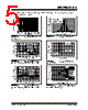


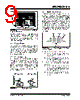


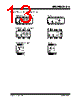


1. General Operating Conditions:
️· Voltage Supply: The amplifier operates with a supply voltage between +1.8V and +5.5V.
️· Temperature Range: Figures reference operating temperatures from -40°C to +125°C.
2. Key Electrical Characteristics (Based on Figures and Notes - these are *not* formal specifications but observations from the plots):
️· Input Offset Voltage (VOS): This is a crucial parameter, and the figures show it's highly dependent on:
- Supply Voltage (VDD): VOS changes with VDD, with values generally shown for 1.8V and 5.5V supplies.
- Common-Mode Input Voltage (VCM): The input offset voltage isn’t constant; it varies with the common-mode voltage applied to the inputs.
- Temperature (TA): There's noticeable drift in VOS with temperature. This is quantified in Figure 2-10, showing a value in µV/°C.
️· Input Bias Current (not explicitly mentioned but inferred): While the plots don't directly show bias current, it's a common parameter for op-amps and likely present.
️· Input Noise Voltage Density: (Figure 12) This is a frequency-dependent characteristic; the lower the frequency the higher the noise.
️· Output Short-Circuit Current: (Figure 13) The short circuit output current varies with temperature.
3. Figure Descriptions (Brief Summaries - See detailed descriptions within the original document):
️· Figure 5: Relationship between the input offset voltage and common mode input voltage at VDD = 1.8V.
️· Figure 6: Relationship between the input offset voltage and common mode input voltage at VDD = 5.5 V.
️· Figure 7: Input Noise Voltage Density vs. Frequency.
️· Figure 10: Input Offset Voltage Drift vs. Temperature (expressed as µV/°C).
️· Figure 11: Input Offset Voltage vs. Output Voltage.
️· Figure 13: Output Short Circuit Current vs. Ambient Temperature.
4. Important Observations & Trends:
️· Temperature Sensitivity: The input offset voltage (VOS) is highly temperature-dependent, which is a critical factor in precision applications. The data includes drift specifications.
️· Common-Mode Dependence: The input offset voltage isn't a fixed value; it's significantly affected by the common-mode input voltage. This suggests careful selection of common-mode biasing is necessary.
️· Supply Voltage Impact: Changing the supply voltage impacts the input offset voltage.
️· Noise Performance: The amplifier exhibits noise performance which decreases as frequency increases.
1. General Operating Conditions:
️· Voltage Supply: The amplifier operates with a supply voltage between +1.8V and +5.5V.
️· Temperature Range: Figures reference operating temperatures from -40°C to +125°C.
2. Key Electrical Characteristics (Based on Figures and Notes - these are *not* formal specifications but observations from the plots):
️· Input Offset Voltage (VOS): This is a crucial parameter, and the figures show it's highly dependent on:
- Supply Voltage (VDD): VOS changes with VDD, with values generally shown for 1.8V and 5.5V supplies.
- Common-Mode Input Voltage (VCM): The input offset voltage isn’t constant; it varies with the common-mode voltage applied to the inputs.
- Temperature (TA): There's noticeable drift in VOS with temperature. This is quantified in Figure 2-10, showing a value in µV/°C.
️· Input Bias Current (not explicitly mentioned but inferred): While the plots don't directly show bias current, it's a common parameter for op-amps and likely present.
️· Input Noise Voltage Density: (Figure 12) This is a frequency-dependent characteristic; the lower the frequency the higher the noise.
️· Output Short-Circuit Current: (Figure 13) The short circuit output current varies with temperature.
3. Figure Descriptions (Brief Summaries - See detailed descriptions within the original document):
️· Figure 5: Relationship between the input offset voltage and common mode input voltage at VDD = 1.8V.
️· Figure 6: Relationship between the input offset voltage and common mode input voltage at VDD = 5.5 V.
️· Figure 7: Input Noise Voltage Density vs. Frequency.
️· Figure 10: Input Offset Voltage Drift vs. Temperature (expressed as µV/°C).
️· Figure 11: Input Offset Voltage vs. Output Voltage.
️· Figure 13: Output Short Circuit Current vs. Ambient Temperature.
4. Important Observations & Trends:
️· Temperature Sensitivity: The input offset voltage (VOS) is highly temperature-dependent, which is a critical factor in precision applications. The data includes drift specifications.
️· Common-Mode Dependence: The input offset voltage isn't a fixed value; it's significantly affected by the common-mode input voltage. This suggests careful selection of common-mode biasing is necessary.
️· Supply Voltage Impact: Changing the supply voltage impacts the input offset voltage.
️· Noise Performance: The amplifier exhibits noise performance which decreases as frequency increases.
| Part No. | MCP6231 |
| Manufacturer | MICROCHIP |
| Size | 477 Kbytes |
| Pages | 28 pages |
| Description | 20 關A, 300 kHz Rail-to-Rail Op Amp |
| ALLDATASHEET vous a-t-il été utile ? [ DONATE ] |
À propos de Alldatasheet | Publicité | Contactez-nous | Politique de confidentialité | Lien vers la fiche technique | Echange de liens | Fabricants All Rights Reserved©Alldatasheet.com |
| Russian : Alldatasheetru.com | Korean : Alldatasheet.co.kr | Spanish : Alldatasheet.es | French : Alldatasheet.fr | Italian : Alldatasheetit.com Portuguese : Alldatasheetpt.com | Polish : Alldatasheet.pl | Vietnamese : Alldatasheet.vn Indian : Alldatasheet.in | Mexican : Alldatasheet.com.mx | British : Alldatasheet.co.uk | New Zealand : Alldatasheet.co.nz |
|
Family Site : ic2ic.com |
icmetro.com |
 French ▼
  English
 Chinese
 German
 Japanese
 Russian
 Korean
 Spanish
 Italian
 Portuguese
 Polish
 Vietnamese
 Indian
 Mexican
 British
 New Zealand